

|
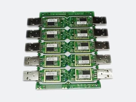
USB wireless card patch processing is a key process to accurately place tiny electronic components on the circuit board to achieve stable signal transmission, and the process is fine and rigorous.
The first is solder paste printing. On the circuit board solder pad that has been cleaned and dried in the early stage, the automatic solder paste printing machine uses steel mesh to accurately control the amount and position of solder paste to ensure uniform printing and consistent thickness, laying the foundation for subsequent component welding.
Then is the component mounting, with the help of high-speed and high-precision Surface Mount Technology mounter, in accordance with the pre-set program, the resistance, capacitor, chip and other types of micro electronic components, from the tray accurately grabbed and affixed to the printed solder paste circuit board corresponding position, each step of the operation is carried out with micron level accuracy, to ensure the accuracy of the mounting.
Then it enters the reflow welding process, and the circuit board with the installed components is sent to the reflow welding furnace. Under the control of the precise temperature curve, the solder paste is melted by heat and cooled and solidified, so that the components and the circuit board solder pad form a solid electrical connection. This process requires extremely high temperature and time control, which directly affects the welding quality.
After the welding is completed, strict AOI automatic optical inspection is carried out, the use of optical imaging technology to scan the circuit board in an all-round way, compared with the preset standards, quickly and accurately identify the component offset, missing parts, short circuit and other defects, and pick out unqualified products for rework.
After testing qualified USB wireless card circuit board, it will be cleaned, remove the residual flux, dust and other impurities in the production process, and then carry out functional testing to verify whether its wireless signal reception and transmission performance is up to standard. Only the products that pass all the testing can enter the final packaging process, and properly package them with anti-static packaging materials. To ensure that the product is not damaged in subsequent transportation and storage, the entire USB wireless card patch processing process is completed.
|
|
USB wireless card patch processing is a key process to accurately place tiny electronic components on the circuit board to achieve stable signal transmission, and the process is fine and rigorous.
The first is solder paste printing. On the circuit board solder pad that has been cleaned and dried in the early stage, the automatic solder paste printing machine uses steel mesh to accurately control the amount and position of solder paste to ensure uniform printing and consistent thickness, laying the foundation for subsequent component welding.
Then is the component mounting, with the help of high-speed and high-precision Surface Mount Technology mounter, in accordance with the pre-set program, the resistance, capacitor, chip and other types of micro electronic components, from the tray accurately grabbed and affixed to the printed solder paste circuit board corresponding position, each step of the operation is carried out with micron level accuracy, to ensure the accuracy of the mounting.
Then it enters the reflow welding process, and the circuit board with the installed components is sent to the reflow welding furnace. Under the control of the precise temperature curve, the solder paste is melted by heat and cooled and solidified, so that the components and the circuit board solder pad form a solid electrical connection. This process requires extremely high temperature and time control, which directly affects the welding quality.
After the welding is completed, strict AOI automatic optical inspection is carried out, the use of optical imaging technology to scan the circuit board in an all-round way, compared with the preset standards, quickly and accurately identify the component offset, missing parts, short circuit and other defects, and pick out unqualified products for rework.
After testing qualified USB wireless card circuit board, it will be cleaned, remove the residual flux, dust and other impurities in the production process, and then carry out functional testing to verify whether its wireless signal reception and transmission performance is up to standard. Only the products that pass all the testing can enter the final packaging process, and properly package them with anti-static packaging materials. To ensure that the product is not damaged in subsequent transportation and storage, the entire USB wireless card patch processing process is completed.


